8-bit Computer from TTL Logic
A breadboard computer built from more than 200 TTL chips with a custom instruction set, a modular architecture, and lab materials used to teach 30 students.
- Problem
- Textbooks explain how a CPU fetches and executes an instruction, but the explanation stays abstract until you can watch the bits move. There was no hands-on computer architecture lab for students to do that.
- Solution
- Built an 8-bit computer on breadboards from more than 200 TTL logic chips, with a custom instruction set and a modular design where the clock, registers, ALU, RAM, program counter, and output display can each be swapped independently. Wrote documentation and lab materials and used the machine to teach 30 students in hands-on workshops.
Overview
What it is: An 8-bit computer built from more than 200 TTL logic chips on breadboards, with a custom instruction set and a 7-segment output display. The clock, registers, ALU, RAM, program counter, and output display are separate modules, so any one of them can be swapped without rebuilding the rest.
Why it matters: Most students meet computer architecture as a diagram. This machine makes the fetch and execute cycle physical: the program counter, the instruction register, the ALU, and the bus between them are all on the bench where you can probe them.
Who it’s for: Students learning digital logic and computer architecture, and anyone teaching those subjects without a lab. The documentation and lab materials were written so a workshop group can follow along at the breadboard.
Impact: The machine and its lab materials were used to teach 30 students in hands-on workshops. Built between May and December 2024 in Zimbabwe.
The Problem
The Challenge
The gap between a block diagram of a CPU and a working CPU is where most students lose the thread. Register transfers, control signals, and timing are hard to reason about when the only feedback is a textbook figure.
Specific issues:
- No hands-on computer architecture lab available
- Simulators hide timing and electrical behaviour
- Students rarely get to see a bus, a control signal, or a clock cycle directly
Who was affected:
- Students learning digital logic and computer organisation
- Anyone teaching those topics without lab equipment
Constraints & Requirements
Technical constraints:
- Built entirely from discrete TTL chips on breadboards, no FPGA or microcontroller
- Each module had to be replaceable on its own so a fault or a lesson could focus on one part
Resource constraints:
- Parts sourced in Zimbabwe, where component availability is limited
- Built by one person between May and December 2024
The Solution
Approach & Methodology
The computer is split into independent modules that share a bus. Each module was built and tested on its own before being connected, which kept debugging local to one breadboard at a time.
Modules:
- Clock
- Registers
- ALU
- RAM
- Program counter
- Output display (7-segment)
Technology Stack
Hardware:
- More than 200 TTL logic chips on breadboards
- 7-segment output display
- Status LEDs on the clock and register modules
Design:
- Custom instruction set
- Modular architecture so each module can be swapped independently
Why this stack:
- TTL chips keep every signal visible and probe-able, which is the whole point for teaching
- Breadboards allow modules to be rebuilt or replaced without redoing the rest of the machine
Key Features
- Modular design: the clock, registers, ALU, RAM, program counter, and output display are separate modules that can be swapped
- Custom instruction set: instructions decoded by the control logic into per-module control signals
- 7-segment output: results are shown on a display driven from the output module
- Documentation and lab materials: written to run hands-on workshops
Technical Highlights
Architecture and the fetch/execute cycle
The modules share one bus. On each clock pulse the control logic chooses which module drives the bus and which module latches from it, so an instruction runs as a short sequence of bus transfers.
The fetch phase is the same for every instruction: the program counter supplies the address, RAM supplies the instruction byte at that address, the instruction register latches it, and the program counter advances. The execute phase depends on the opcode now sitting in the instruction register, which the control logic decodes into the control signals for the remaining steps, for example moving a value from RAM into a register or putting an ALU result on the bus.
The table below is illustrative only. It shows the shape of a microcode-style control sequence for a “load register from memory” instruction on a machine of this kind, not the exact signals of the finished build.
| Step | Phase | Bus source | Bus destination | Other |
|---|---|---|---|---|
| 0 | Fetch | Program counter | Memory address | |
| 1 | Fetch | RAM | Instruction register | Advance program counter |
| 2 | Execute | Instruction register (operand) | Memory address | |
| 3 | Execute | RAM | Register |
Illustrative microcode-style sequence. The real control logic differs in its step count and signal names.
Build Gallery
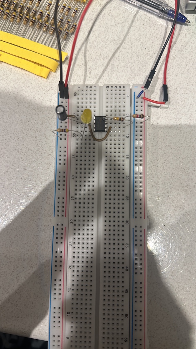 First breadboard, May 2024.
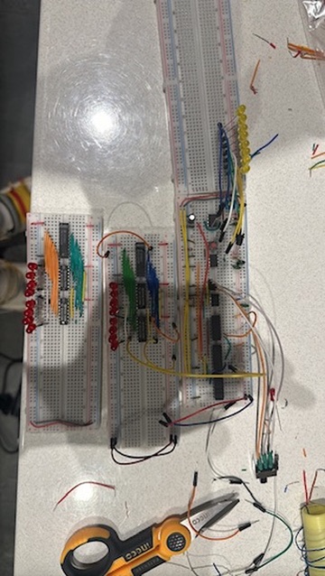 Clock and register LEDs, June 2024.
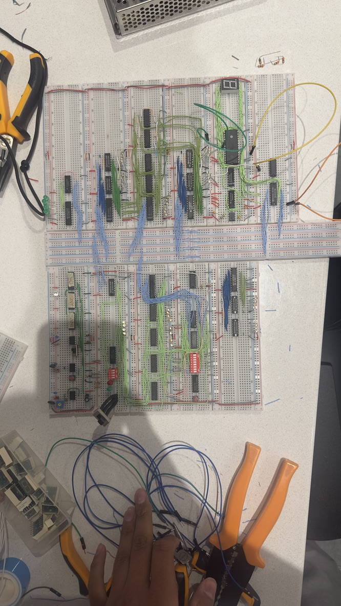 Bus and registers, September 2024.
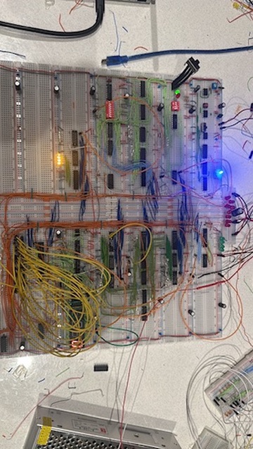 ALU wiring, September 2024.
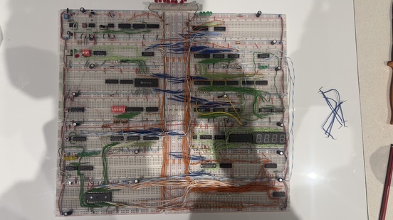 Full board from above, September 2024.
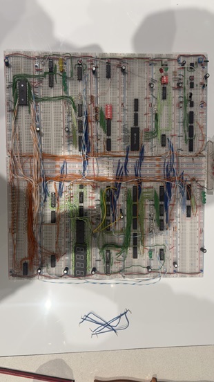 Full board from the side, September 2024.
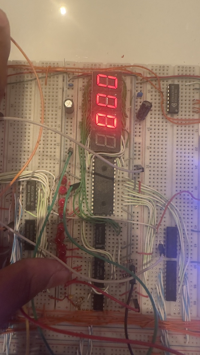 Seven-segment output display, September 2024.
Process & Timeline
The build ran from May to December 2024. The photo dates give the rough order:
- May 2024: first breadboard
- June 2024: clock and register modules with status LEDs
- September 2024: bus, registers, ALU, and the full board with the 7-segment output display
- By December 2024: custom instruction set, documentation and lab materials, and workshops for 30 students
Challenges & Solutions
Challenge 1: Debugging across 200+ chips
The Problem: With this many chips and wires on breadboards, a single loose connection can corrupt a bus transfer and the symptom shows up far from the cause.
The Solution: Keep modules independent. Each module was built and tested on its own breadboard before it joined the bus, so a fault could be isolated to one board.
What I learned: Modularity is a debugging tool, not just a design nicety.
Challenge 2: Teaching with it
The Problem: A machine that only its builder can operate does not teach anyone.
The Solution: Wrote documentation and lab materials that walk a group through the modules and the fetch/execute cycle, and ran hands-on workshops with the machine on the bench.
What I learned: Writing the lab materials forced a clearer description of the control sequence than the wiring alone gave me.
Results & Metrics
- More than 200 TTL chips on breadboards
- Six swappable modules: clock, registers, ALU, RAM, program counter, output display
- Custom instruction set
- 7-segment output display
- 30 students taught in hands-on workshops using the documentation and lab materials
- Built May to December 2024
Learnings
- Building each module independently and connecting them over one bus made the project tractable for one person
- Documentation written for students doubled as the clearest specification of the machine
- A physical machine holds a workshop’s attention in a way a simulator does not
Links & Resources
- Build photos are in the gallery above
Completed: December 15, 2024